

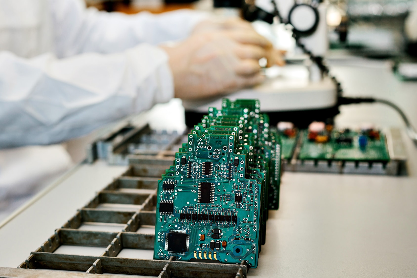
Printed circuit boards (PCBs) are essential components in many electronics devices, from smartphones to aerospace equipment. As a PCB designer or manufacturer, it’s crucial to understand the PCB fabrication process, which involves turning a design into a physical PCB. In this article, we’ll provide an overview of the PCB fabrication process, from preparing the design to final inspection and testing.
Preparing the Design
The first step in the PCB fabrication process is to prepare the design. This involves creating a file in a specific format, determining the layer stackup, and panelizing the design. The file is then sent to the PCB manufacturer, who will use it to generate the film.
Film Generation
The next step is film generation. The printed circuit board fabricator uses the design file to create film, which is a negative of the PCB image. The film is then used to create the PCB image on the photoresist.
Imaging and Developing
The photoresist-coated copper board is exposed to UV light through the film, which hardens the photoresist in the areas where the copper traces and pads should be. The board is then developed to remove the unexposed photoresist.
Etching and Stripping
The PCB is etched to remove the unprotected copper, leaving only the copper that’s protected by the photoresist. Once the copper is etched away, the photoresist is stripped away, revealing the final copper traces and pads.
Drilling and Plating
The PCB is drilled to create the necessary holes for components and vias. The manufacturer can add additional copper layers or create vias through plating.
Solder Mask and Silk Screen
Solder mask and silk screen layers are added to the PCB to protect the copper traces and add text and graphics. The solder mask is a protective coating applied over the copper, while the silk screen is used to print text and graphics.
Final Inspection and Testing
The final step in the PCB fabrication process is the inspection and testing. The manufacturer inspects the PCB for defects, such as missing or shorted traces, and tests the electrical connections to ensure they’re functioning properly.
Conclusion
Understanding the PCB fabrication process is crucial for both PCB designers and manufacturers. By following these steps, you can turn a design into a functional PCB that can be used in a variety of electronic devices. If you’re new to the process, be sure to work with an experienced PCB fabricator who can guide you through the process and ensure a high-quality result.